Imported PCBs worth ₹40,000 crore to be manufactured in India; Jewar to emerge as a major electronics manufacturing hub : Ashwini Vaishnaw
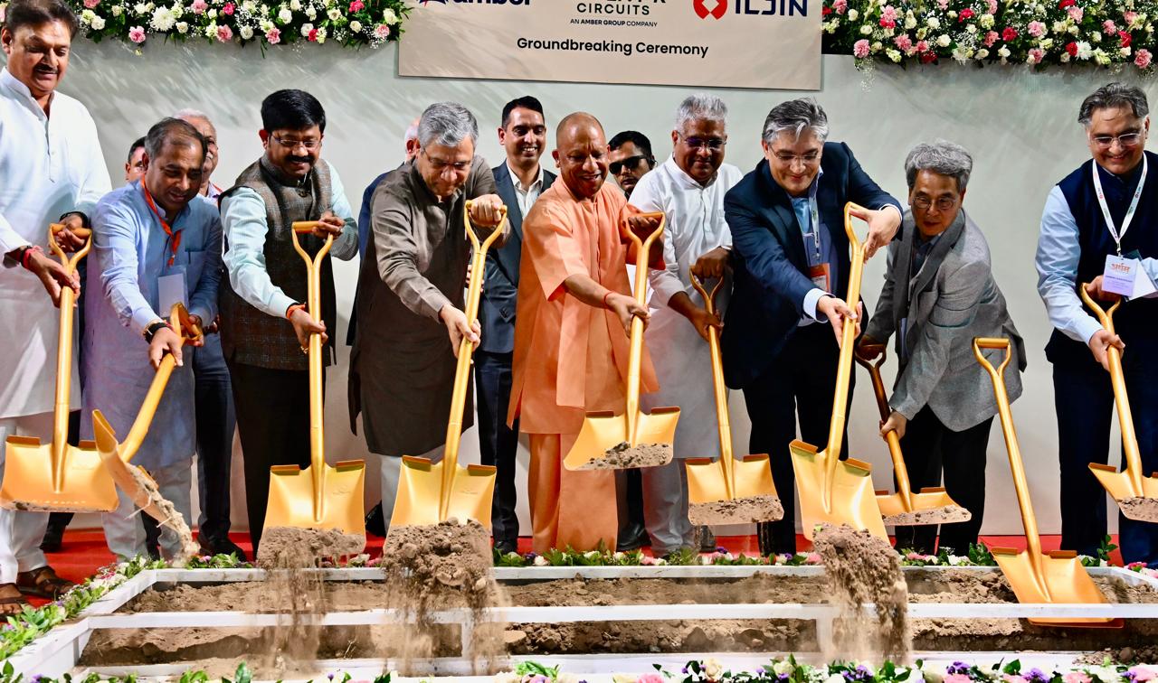
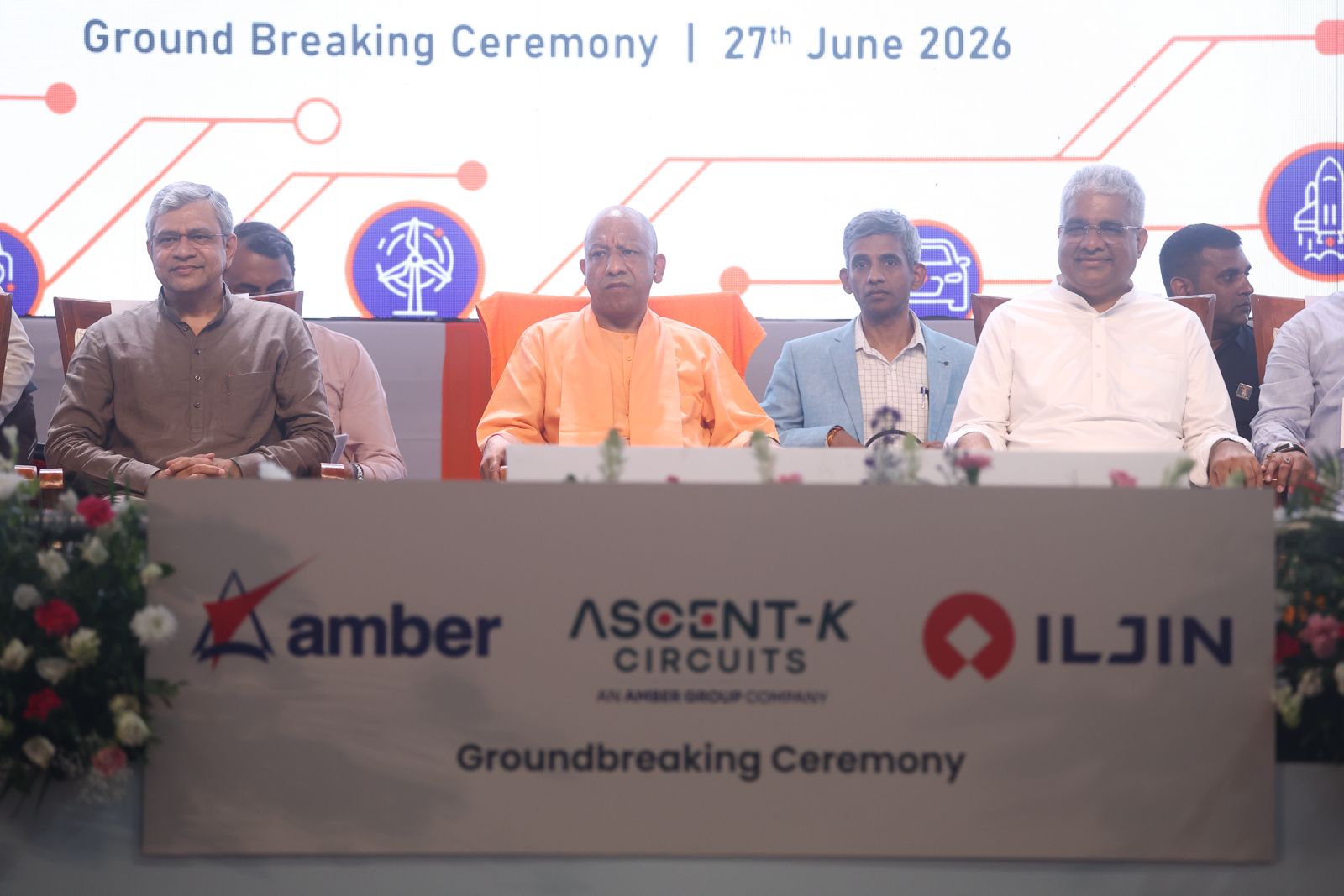
NEW DELHI : Chief Minister of Uttar Pradesh, Shri Yogi Adityanath and Union Minister for Electronics & IT, Railways and Information & Broadcasting, Shri Ashwini Vaishnaw jointly laid the foundation stones for two major electronics manufacturing projects involving an investment of approximately ₹6,750 crore at Yamuna City, Jewar, in Gautam Buddha Nagar district of Uttar Pradesh.
Addressing the gathering, Shri Ashwini Vaishnaw said that Jewar is poised to emerge as one of India’s leading hubs for electronics and semiconductor manufacturing in the coming years.
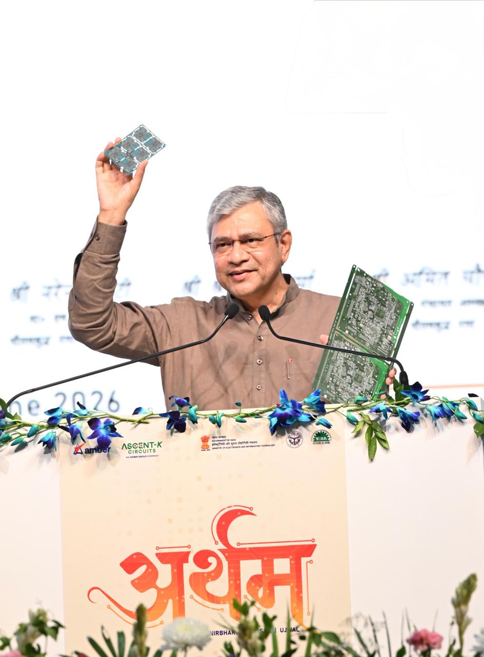
Explaining the significance of the projects, Shri Ashwini Vaishnaw said that the facilities would manufacture advanced multi-layer Printed Circuit Boards (PCBs), one of the most critical components of modern electronic devices. He noted that these highly sophisticated PCBs, comprising up to 20–22 layers of integrated circuitry within an extremely thin structure, form the backbone of today’s electronics industry. He said that PCBs worth nearly ₹40,000 crore, which were earlier imported into the country, will now be manufactured domestically, with Jewar emerging as a major production centre.
Union Minister further said that, following the development of the semiconductor ecosystem, Jewar is now poised to become a major centre for electronics manufacturing as well. He expressed confidence that several new electronics manufacturing projects would be established in Uttar Pradesh, enabling the State to emerge as one of the country’s leading electronics and semiconductor manufacturing hubs. He said that the projects would strengthen India’s journey towards technological self-reliance and give fresh momentum to the vision of Aatmanirbhar Bharat by expanding domestic manufacturing capabilities across the electronics value chain.
Highlighting the transformative impact of infrastructure, Shri Ashwini Vaishnaw said that the proposed Delhi–Lucknow–Varanasi–Patna–Siliguri Bullet Train corridor will redefine connectivity across Uttar Pradesh and act as a catalyst for industrial and economic growth. He noted that world-class transport infrastructure, coupled with a robust electronics manufacturing ecosystem, will significantly enhance the State’s attractiveness as an investment destination.
During the programme, Chief Minister Shri Yogi Adityanath also laid the foundation stone of the first industrial unit to be established in the Electronics Manufacturing Cluster (EMC) located in Sector-10 of the Yamuna Expressway Industrial Development Authority (YEIDA).
The Electronics Manufacturing Cluster is being developed over an area of 206 acres at an estimated cost of approximately ₹417 crore with the support of the Government of India, including a Central Government contribution of ₹144 crore. The project is expected to strengthen Uttar Pradesh’s position as a leading electronics manufacturing destination and promote investment in high-value electronics manufacturing.
Building India’s Semiconductor Ecosystem
The India Semiconductor Mission (ISM), launched under the Semicon India Programme, is building a comprehensive semiconductor and electronics manufacturing ecosystem in the country. As of June 2026, the Government has approved 12 semiconductor manufacturing projects with an investment pipeline of approximately ₹1.64 lakh crore, comprising one semiconductor fabrication unit, two compound semiconductor fabrication units and nine semiconductor packaging units.
The Mission is also strengthening India’s semiconductor design ecosystem through the Design Linked Incentive (DLI) Scheme. So far, 24 design projects are being supported, 105 companies have received access to advanced Electronic Design Automation (EDA) tools, and 23 chip tape-outs have been completed at various foundries, including advanced technology nodes. Announced in the Union Budget 2026–27, India Semiconductor Mission 2.0 aims to further strengthen the ecosystem by promoting semiconductor equipment and materials, indigenous intellectual property, resilient supply chains and advanced manufacturing capabilities, reinforcing India’s emergence as a trusted global semiconductor hub.